XREG-010 Overheating Flyback Diode Fix
I upgraded the test bench with 6 alternator rotors (a nice eBay find), which can be wired in parallel to produce adjustable load of the proper resistance and inductance for the regulator. This allows steady-state testing to the extremes of the regulator’s claimed values (48V-class voltages, 10 amp fields), which could previously only be checked in short transients.
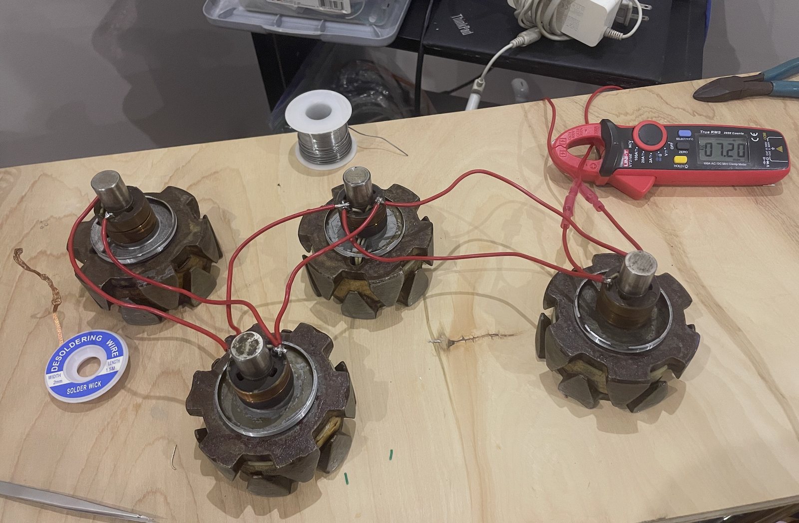
The flyback diode overheats
Right away, D5, the flyback diode for P type mode, was discovered to overheat at high-voltage, high-current fields. Its limit is 150C junction temperature. Not good!
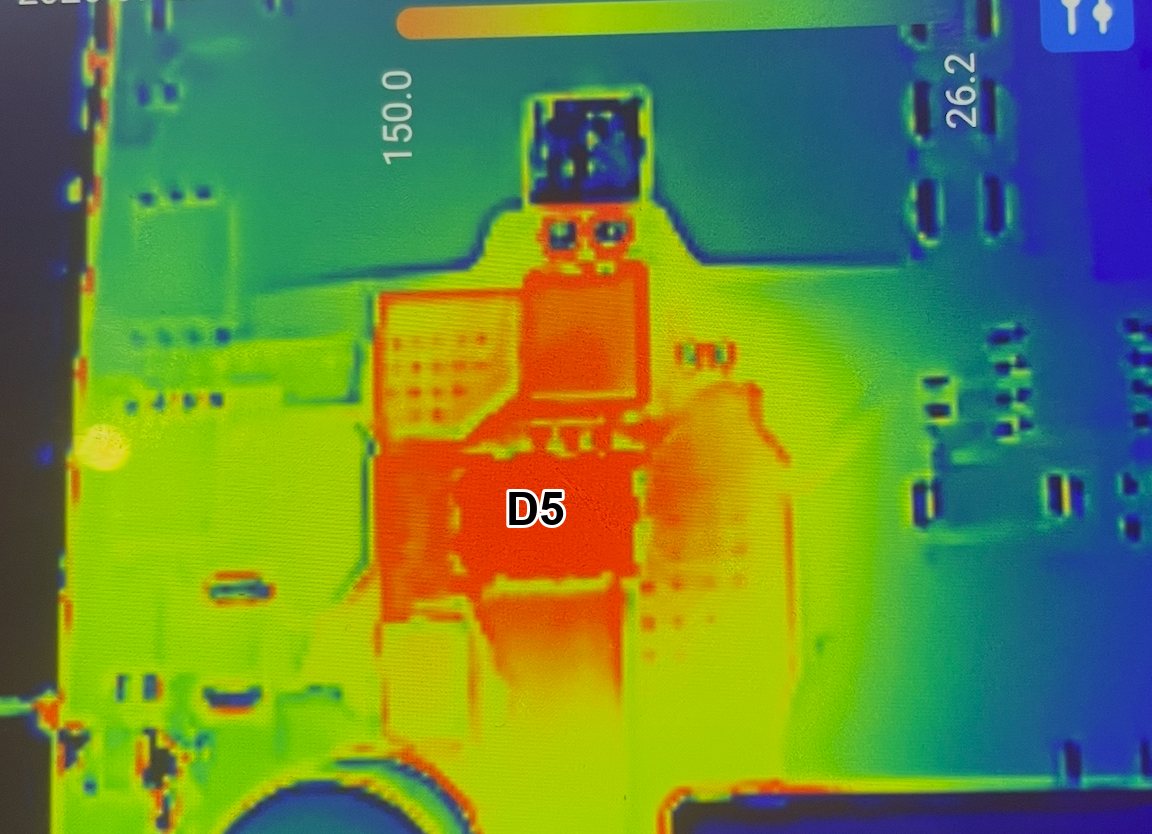
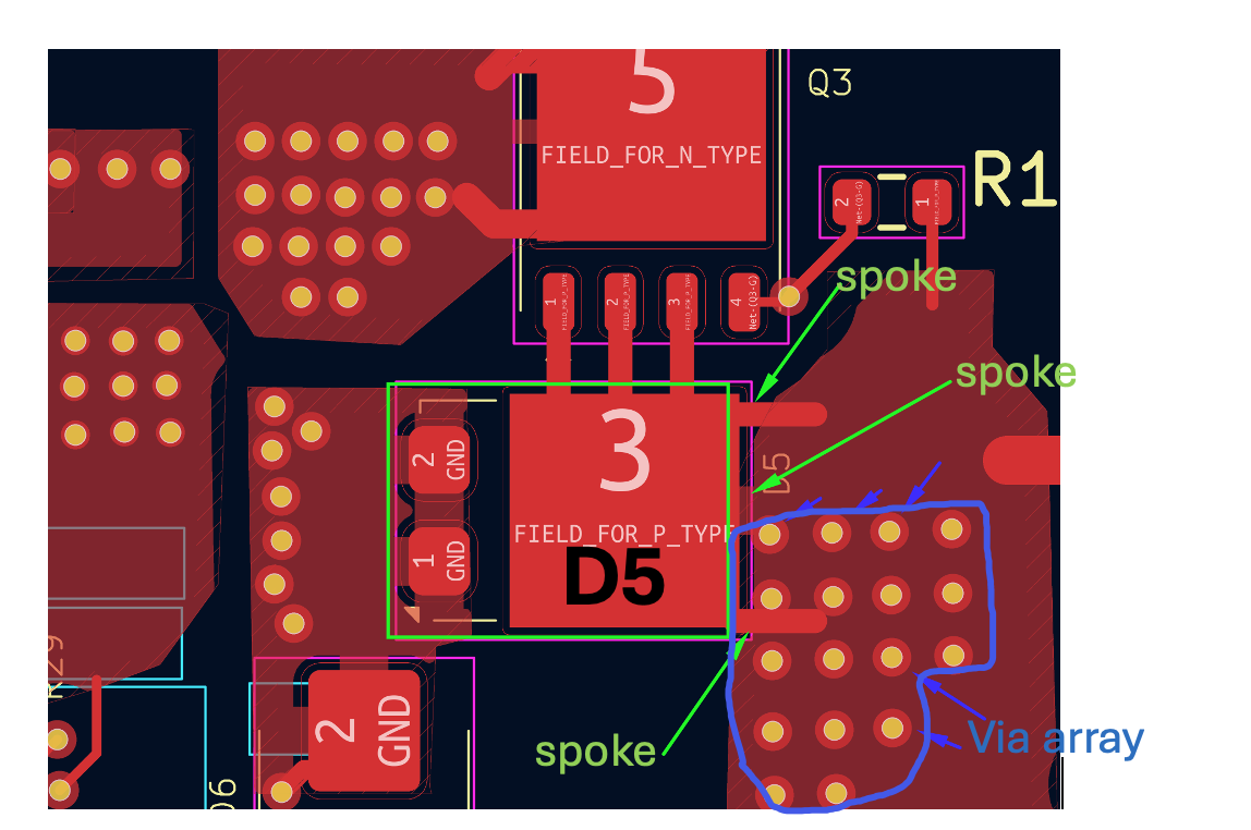
The fault is carelessness in my PCB layout. The default footprint for these diodes includes thermal spokes, shown above by green arrows. The spokes connect the field solder pad “3” to the copper pour to the right. The copper pour dissipates heat well thanks to its own size and array of vias (blue arrows) that transfer heat to other layers of the PCB. Thermal spokes are a great convenience for hand soldering, because they make the pads easier to heat up, but for the same reason they’re terrible for cooling, and should not be used on heavily loaded power components like this flyback diode. Hand soldering convenience is a moot point, we should never have to remove this thing if it's engineered correctly in the first place.The thermal camera image shows a large temperature delta between D5 and the copper pour to the right. In contrast to what's shown here, the ideal cooling scenario would be to put the vias directly under the diode’s pad, and also to connect the copper pour without spokes. If that’s not enough, the thickness of the copper in the PCB layers can also be increased, at the expense of about a couple dollars per board.
But what to do about V9? They're already shipping and need some kind of upgraded cooling to keep D5 below 150C at its junction, at the extremes of what a customer might need, and to meet the advertised specs. And a secondary problem: how can temperature even be measured when inside the enclosure, which is expected to provide unwanted insulation, with the thermal camera blocked by wood?
A diode thermometer
I put the problem to Claude and it came up with a great answer: use the voltage drop (Vf) of our overheating diode, when loaded, which is easily measurable, to calculate temperature. This is a standard technique, but normally calibrated using a toaster oven and a tiny test current. Below is a unique interpretation, which makes use of a series of calibration points at varying voltages, duty cycles, and currents, and some fancy data fitting. I used this exactly:
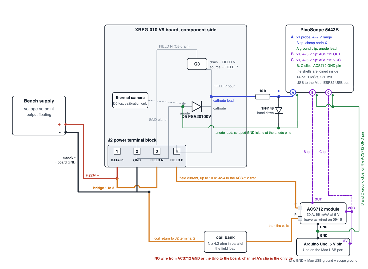
Here is Vf, the diode voltage drop in a single test point, as measured by Channel A:
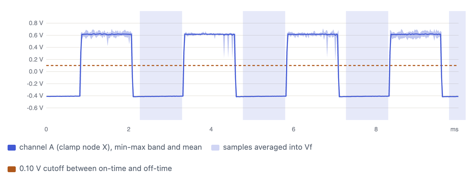
The added 1N4148 diode clips the positive voltage at about 0.6V, allowing a tight oscilloscope range for best resolution. The flat bottom of each off-time (about -0.4V here) is Vf. The scope reads it negative because its ground clip is on D5’s anode. Flyback current is caused by the inductance of the field coil(s), which wants to keep current flowing every time the 400 Hz PWM turns the field off, and the only path for it is from ground, up through D5, and back into the field.
Calibration results
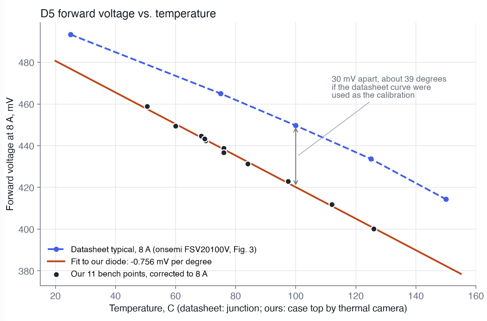
Near perfect and very usable relationship between voltage drop and case top temperature! (Our line looks better than the datasheet, but I’m not sure linear is the theoretical truth...)
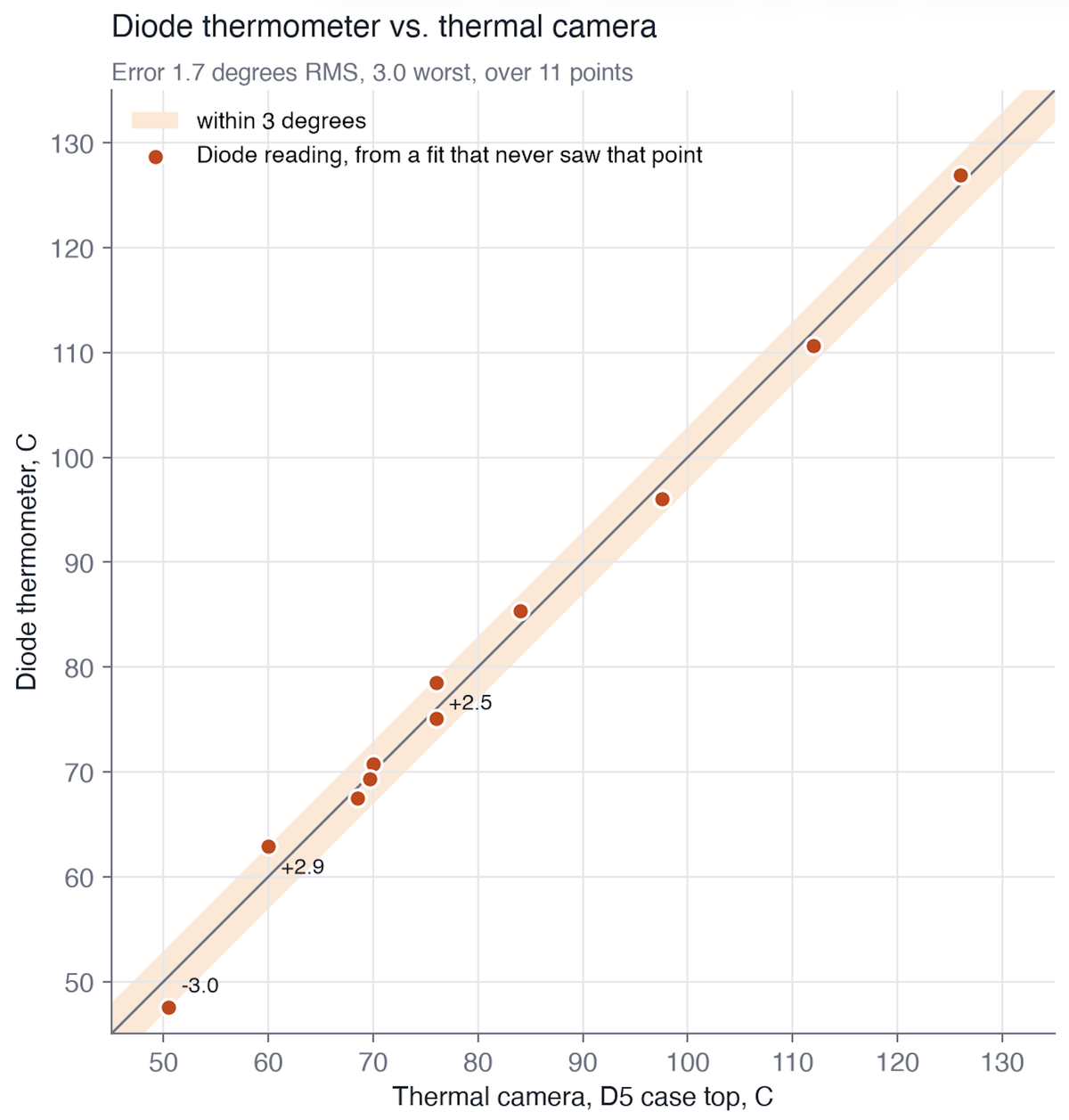
Our “diode thermometer” is within 3 degrees of the camera for all tested points:
The next step was to quantify the steady-state temperature for a given power level, in the enclosure, at tonight's 22C ambient temperature.
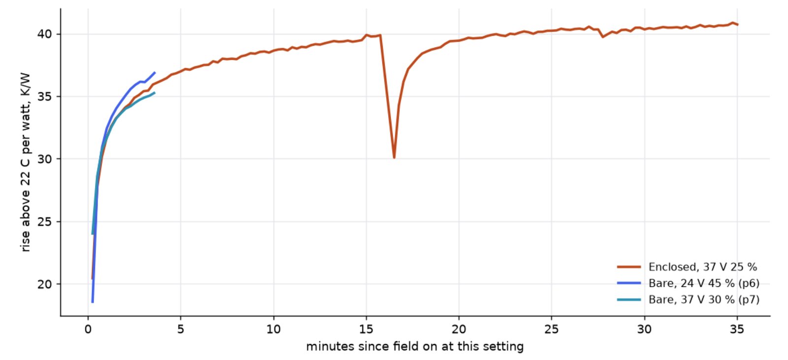
The large dip was a “zero check” mid-run, ignore. The important result, based on the limited data collected so far, is that the enclosure does not seem to provide much insulation, having enough venting out the bottom and conduction thru the wood to not provide a meaningful bottleneck. To confirm this, the “bare board” needs to run a full 35 minutes, but based on the rise rate of each in the first couple minutes, it’s not going to be dramatically different.
What are worst case scenarios?
The junction temperature rise above ambient = the watts in D5 times the thermal resistance to the air. Voltage and duty cycle only matter in that they change power in D5. There are two power sources. During the PWM off-time, D5 carries the whole field current, so it burns Vf x amps x the fraction of time the field is off. During the on-time, D5 is blocking the full battery voltage and leaks a little current backwards, so it burns volts x leakage x the fraction of time the field is on. Switching losses are negligible at 400 Hz.
Off-time Vf × field amps × (1 − duty)
On-time battery volts × leakage × duty
Higher voltage is worse for the same field current, because the regulator needs a lower duty cycle to make that current, and D5 carries it for a bigger share of every cycle. At 58V with our (4) bench rotors, 10 amps needs about 23% duty, so D5 is carrying 10 amps 77% of the time. Note: a “48V rotor” on a 48V system runs about the same duty as a 12V rotor on a 12V system. A 12V rotor on a 48V system is the worst case, so that’s our design assumption here.
With one rotor on one battery voltage, the current goes up as the duty goes up, and D5’s loss (amps x off-time) peaks at 50% duty. With our 1.3 ohm bench load at 58V, that peak would be at about 22 amps, so in the real operating range the loss only climbs with current.
Leakage is the nasty one near the limit. The FSV20100V datasheet shows about 10mA of leakage at 58V and 125C, and about 30mA at 150C. That’s 0.3 to 0.4 watts at 58V, and it rises with temperature, which raises the temperature, which raises the leakage.
How many field amps before the junction hits 150C, in the enclosure, at 50C ambient, for each voltage class?
14.5VPass
Never. The worst case is about 1.1 watts at 5.6 amps, far below the limit.
29VFail
About 8 to 9 amps, missing the 10 amp target. FAIL.
58VFail
About 6.5 amps. At 10 amps D5 would be making about 3.7 watts, well past the limit. FAIL.
At 22C ambient, 58V gets to about 8 amps and 29V clears 10 amps.
Assumptions
- The junction runs 1.5 degrees per watt hotter than the case top, which is a model number, not a measurement.
- The leakage comes from the datasheet’s typical curves.
- There is only one steady run in the enclosure so far, at 2 watts, on our 1.3 ohm bench load.
A few more tests (not run yet) will confirm the above, but we already know well enough that a fix is needed, and we have enough information to model it before ordering anything.
A graphite thermal spreader
After much research and modeling, the most convenient way I found to provide better cooling to D5 is a Thermal Spreader. There are many companies making graphite spreaders, which transfer heat super efficiently in the X/Y direction (about 3 times better than copper for the NeoNxGen grade: 1100 W/mK, against 400 for copper).
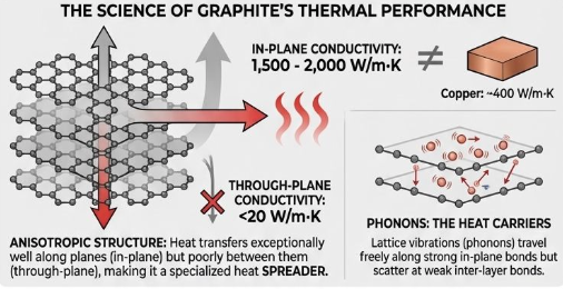
The most practical option I found was NeoGraf Solutions with their “NeoNxGen.” It is a graphite spreader, but with unique advantages.
- Flexibility: NeoGraf rates it for 200,000 bends at a 4mm radius with no change in performance.
- Electrically Insulating and Sticky: It can be purchased with a thin plastic layer, and an adhesive layer (much easier than dealing with separate glue issues).
- DIY friendly: It can be cut with scissors. So the entire rework could be cutting out a sticker that fits, and pressing it on.
Sounds great!
Starting with the KiCad files, test data, and various datasheets, Claude created a thermal model of the problem, including all the board layers, the vias, convection, conduction, radiation, the innards of D5 after I provided teardown photos, about 50 different options for thermal spreaders, the works…
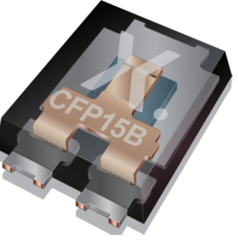
The main concern was how much of a thermal path could exist thru the top 0.4mm or so of case material on top of the internal copper, which is a poor conductor compared to the engineered heat path out the bottom's solder pads. But simulation results mercifully show a graphite spreader is still very effective.
The following numbers are for a single layer of NeoNxGen N-270 (0.27mm thick), with a thin plastic film on top and film plus adhesive on the bottom. The front piece covers D5 and Q3, and the back piece is a 37 x 61mm rectangle on the bottom of the board, behind D5. Same conditions as before: in the enclosure, 50C ambient, the 1.3 ohm bench load (simulating massive alternator).
No spreaderFail
42.5 C/W
At 58V and 10 amps the junction is well over 150C, and the limit is about 6.5 amps. We know from before: FAIL.
Front spreader onlyBarely
26 C/W, 38% cut
58V at 10 amps runs the junction at 144C. Passes, barely.
Both sides spreaderPass
25 C/W, 42% cut
58V at 10 amps is 138C, and 29V at 10 amps is 111C. Pass.
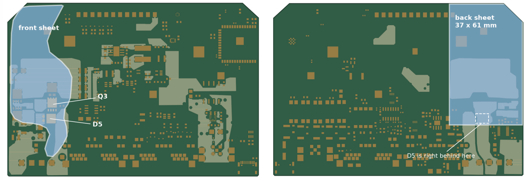
The front sheet does most of the work because it sits right on top of D5. The back sheet adds another 6 degrees of margin at 58V. The sheets themselves run about 30-40 degrees above ambient, so 80-90C at 50C ambient, well under the 150C rating of the film and adhesive.
This assumes the enclosure doesn’t change how much the sheets help, which obviously must be tested next. Hopefully that's all for P- type max power validation. N type is another story, coming soon.
← Back to X Engineering